CMOS gate as a linear amplifier
By David Stonier-Gibson
There are times when you are making an essentially all-digital circuit, but need a little bit of linear amplification. Examples of this would be a microphone pre-amp for a sound triggered switch, or a photodiode pulse pre-amplifier. I have used this several times throughout my career, when a left over gate can be used instead of having to add another chip to the design. It works with any inverting gate, meaning NAND, NOR or NOT (usually called inverter). NAND and NORs have more than one input. Use one of the inputs, then tie the others to ground for NORs and + supply for NANDs.
Note: This trick will only work with unbuffered CMOS gates or inverters. That means, for 4000-series chips, the ones with a U suffix, such as 4002UB. For 74 series chips it means ones with a single 'C' in the part number, such as 74C04 (but not 74HC04. It also won't work with Schmitt trigger parts such as 40106UB or 74C14. And it certainly won't work with TTL chips like 74LS04, 7404, 74S04).
The simplest circuit
I am illustrating my circuits with an inverter, but they will also work with NAND and NOR gates (see above).
I am illustrating my circuits with an inverter, but they will also work with NAND and NOR gates (see above).
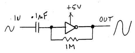
Oops, I forgot to draw the ground (power) connection!
This circuit will work well with a fairly low impedance signal source (say an electret microphone). The voltage gain will depend on the specific chip you are using, and on the supply voltage. I used a 4069UB from Texas instruments, and recorded a gain of about 40 with a 5V suppy. You can go to higher supply voltages, up to 15V with 4xxx and 74Cxx chips - more on this below
This circuit will work well with a fairly low impedance signal source (say an electret microphone). The voltage gain will depend on the specific chip you are using, and on the supply voltage. I used a 4069UB from Texas instruments, and recorded a gain of about 40 with a 5V suppy. You can go to higher supply voltages, up to 15V with 4xxx and 74Cxx chips - more on this below
|
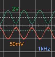
The oscillograph shows the input (bottom, red) at 50mV/div, so we have about 50mVpp. The top/green trace is the output, about 2Vpp, which is about as much as I could get out of it before getting visible distortion. I am not sure what the "fuzz" is on the input trace. I used my nScope for this, and I am pretty sure it is simply noise in the nScope. The low frequency cutoff (-3dB) point will be the capacitor versus the sum of the source impedance and amplifier input impedance. If the source impedance is very low, we can just use the amplifier input impedance of 500K/40, or about 25K, giving a cutoff of about 65Hz.
|
The way this works is that the 1M resistor provides DC feedback, and ensures that the circuit will stabilise itself to a quiescent voltage of about half the supply voltage. The signal to be amplified has to be couple via a capacitor, to avoid disturbing the DC operating point. It's best to not use an electrolytic capacitor, because leakage currents will disturb the operating point.
The input impedance will be roughly the feedback resistor (1M) divided by the gain of the chip (in my case, 40), so about 25K.
The input impedance will be roughly the feedback resistor (1M) divided by the gain of the chip (in my case, 40), so about 25K.
|
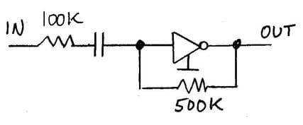
A little fancier
If the "raw" gain of the chip is too much, you can make a crude approximation to a "proper" opamp configuration. If this was a proper opamp, the gain would be 500K/100K = 5. But it's not a proper opamp, so we get less gain. The "gain error" is 5/40 or 1/8, so we will get 1/8 less gain than we want. I'm not going to do the full math for you! |
|
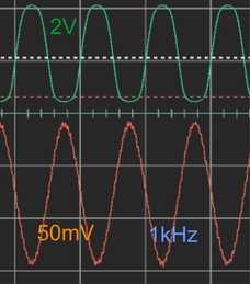
Adding the 100K resistor introduces some negative feedback. The will allow us to get a bit more output voltage swing for a given distortion level, but only a bit. Here's what it looks like with just under 4Vpp output.
What value capacitor? I hear you ask. The capacitor value will determine the low frequency cutoff. It is "working against" the 100K resistor. 0.1uF would give a cutoff (-3bB point) of 1/(2*pi*R*C) = 16Hz. Actually, it will be a bit lower than that because we should add in the amplifier effective input impedance of ~12K, but remember these circuits are pretty rough and ready.
What value capacitor? I hear you ask. The capacitor value will determine the low frequency cutoff. It is "working against" the 100K resistor. 0.1uF would give a cutoff (-3bB point) of 1/(2*pi*R*C) = 16Hz. Actually, it will be a bit lower than that because we should add in the amplifier effective input impedance of ~12K, but remember these circuits are pretty rough and ready.
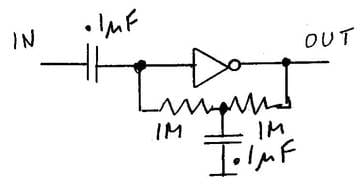
Increasing the input impedance
The first circuit above has in input impedance of around 25K. The second is about 100K, but at the cost of less gain. Suppose I want maxium gain and a high input impedance?
The first circuit above has in input impedance of around 25K. The second is about 100K, but at the cost of less gain. Suppose I want maxium gain and a high input impedance?
|
IF I split the feedback resistor in two, then connect the junction of them to ground via a capacitor, I effectively short out or cancel the negative feedback at all AC frequencies where the capacitor is a low impedance. So now I get the DC stability from the resistive (DC) feedback, but the full gain of the chip at AC. At the same time, the input impedance becomes just the left-hand resistor.
|
|
Just a tad more theory
CMOS gates or inverters are really only designed to have two output states: On or off. In practice the circuits will transition bewteen those two extreme states as the input voltage varies.
CMOS gates or inverters are really only designed to have two output states: On or off. In practice the circuits will transition bewteen those two extreme states as the input voltage varies.
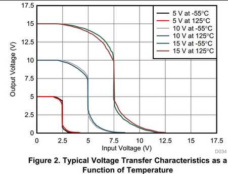
Here is an extract from the data sheet of the chip I used on this page, Texs Instruments 4069UB. It is a graph of output voltage versus input voltage at 3 different supply voltages and two temperature extremes. You can see that for 0V in, the output is at the supply voltage. Then, as the input voltage increases, there is a range where the output starts to slowly change. Then, as the input voltage increases further, the output starts to change more rapidly until it gets to a point where it makes a big change for only a tiny change in the input. Then the reverse happens, and the output starts to more gently approach 0V.
Now, the "gain" of an amplifier is the change in output divided by the change in input. It is the slope of the graph. The steeper the graph, the higher the gain. When I measured a gain of 40 (with a 5V supply, by the way), I was really measuring that steep bit in the middle. Outside that range, the gain is less than 40. In fact, at either end it is exactly zero. And on those "soft corners", the gain of our amplifier will be low, and the output waveform will be severely distorted. So don't expect to use one of these circuits in a precision instrument or in your HiFi system.
What about supply voltages greater than 5V?
These circuits are operating the CMOS gate in the middle of its output swing, when the current drawn by the gaet is at its maximum. The table shows typical current draw and dissipation (heat generation) for one gate, versus supply voltage. You can see that at 5V it's running cool. But at 15V there's quite a bit of heat being generated.
These circuits are operating the CMOS gate in the middle of its output swing, when the current drawn by the gaet is at its maximum. The table shows typical current draw and dissipation (heat generation) for one gate, versus supply voltage. You can see that at 5V it's running cool. But at 15V there's quite a bit of heat being generated.
|
If you tried to use all 6 inverters in a 4069UB as amplifiers at 15V, the chip would be dissipating well over one watt, and would overheat and eventually die. The Texas data sheet suggest you can dissipate up to 500mW in the whole chip, but I would never do that to a CMOS chip. I would stick within 100-200mW tops. If the chip gets too hot the input leakage currents are likely to increase, and upset the DC stability.
|
Must it be unbuffered CMOS?
Simply put, normal buffered CMOS has far too much gain. In an operational amplifier, the more gain the better. But a buffered CMOS gate was never designed for linear (analogue) use, and its frequency response means it is essentially impossible to make it stable with negative feedback. I did actually try a 74HC04 for this article, and wound up with a 240MHz oscillator drawing over a watt from the power supply and getting nice and hot. That oscillation is something you would have trouble detecting without a very good oscillscope and a lot of experience.
Simply put, normal buffered CMOS has far too much gain. In an operational amplifier, the more gain the better. But a buffered CMOS gate was never designed for linear (analogue) use, and its frequency response means it is essentially impossible to make it stable with negative feedback. I did actually try a 74HC04 for this article, and wound up with a 240MHz oscillator drawing over a watt from the power supply and getting nice and hot. That oscillation is something you would have trouble detecting without a very good oscillscope and a lot of experience.
